
Peking University-Backed SpinPU Unveils Inference Chip Targeting 2000 Tokens/s
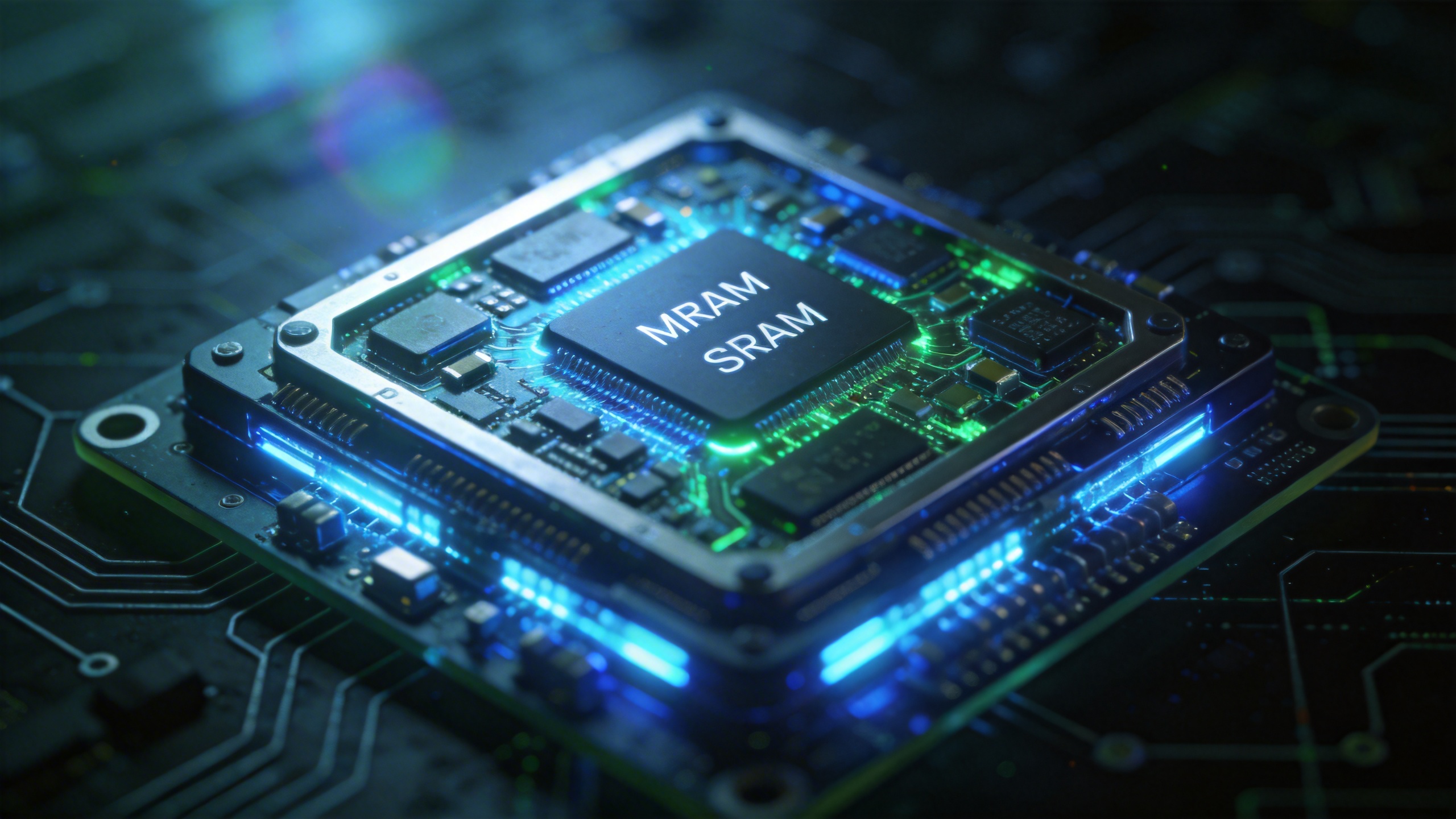
A Chinese startup backed by Peking University, SpinPU Technology, announced it has secured tens of millions of yuan in financing and completed testing of its initial chip sample. The company, which specializes in ultra-high bandwidth streaming inference, aims to achieve 2000 Tokens/s with its next-generation hybrid "MRAM+SRAM" architecture. This development emerges as the inference chip landscape undergoes significant shifts, including reports of NVIDIA's substantial engagement with Groq.
SpinPU Technology's announcement comes ahead of NVIDIA's GTC 2026 conference, an event widely anticipated to highlight the industry's pivot toward inference computing, particularly with the rise of Agents and embodied AI. NVIDIA's reported $20 billion move to acquire or partner with Groq, a North American inference chip company, underscores the increasing importance of specialized inference solutions. Traditional GPUs, while powerful for parallel computing in training, face limitations such as the "memory wall" and dynamic scheduling latency when handling streaming large model inference.

NVIDIA GTC conference stage with a large screen and audience, highlighting industry events.
Qigao Capital and Saiyi Industry Fund led SpinPU Technology's latest funding round, with Yuanhe Capital acting as the exclusive financial advisor. The company stated that its first sample chip achieved a unit area bandwidth of 100 GB/s/mm², validating its core functions and technical approach.
Architectural Approach to Inference

Visual metaphor of data flowing deterministically on a microchip, representing 'assembly line mode' processing.
SpinPU Technology's approach diverges from traditional GPU architectures, aligning with principles seen in Groq's Language Processing Units (LPUs). The company emphasizes a streaming, high-bandwidth architecture with on-chip weight storage, moving away from hardware scheduling. Internally, this is described as an "assembly line mode" rather than the "piecework factory mode" of GPUs.
The company's design focuses on:
Algorithm-guided Determinism: SpinPU employs algorithm-guided, decode-specific, and deterministic data flow planning for neural network forward propagation. This aims to ensure precise scheduling and processing, eliminating latency jitter from dynamic resource contention.
Operator-oriented Data Path: The chip's internal space is divided into functional blocks optimized for Transformer models, including on-chip weight storage, GEMV (General Matrix-Vector Multiplication) computing units, and vector computing units. This design is intended to create an efficient pipeline for weight reading and computation.
Bandwidth Optimization: SpinPU's strategy centers on maximizing bandwidth utilization, a critical factor in large model inference where throughput is often bandwidth-bound rather than compute-bound.
The achieved unit area bandwidth of 100 GB/s/mm² is a key metric for streaming inference architectures, directly influencing inference speed. This figure suggests a higher density weight access capability per unit area compared to traditional architectures and even some specialized inference solutions.

Abstract visualization of glowing data streams converging, symbolizing optimized bandwidth and high throughput.
Hybrid Memory for Enhanced Performance
SpinPU Technology's upcoming chip is slated to feature a hybrid "on-chip MRAM + SRAM" storage architecture. This design aims to address the limitations of pure SRAM solutions, which, while fast, have low density and can necessitate large clusters for substantial models.
SRAM (Static Random Access Memory): Utilized for high-speed caching and intermediate variable computation, ensuring low latency.
MRAM (Magnetic Random Access Memory): A non-volatile memory type offering speeds close to SRAM but with significantly higher density and lower power consumption.
This hybrid approach is intended to increase the model capacity storage density of a single chip while maintaining the benefits of a deterministic streaming architecture. SpinPU targets an extreme performance of 2000 Tokens/s, a substantial increase over current market speeds for conversational model inference, which typically range from 30-50 Tokens/s. Such performance could enable real-time applications in areas like embodied AI, simultaneous interpretation, and complex multi-agent planning.

Modern architecture on the Peking University campus, representing its academic origins.
Peking University Origins and Strategic Timing
SpinPU Technology was established in August 2023, with its founding team originating from the "Peking University Magnetism Center." The team combines academic expertise with engineering experience in new memory technologies, such as MRAM, and compute-in-memory architecture integration. This background is cited as crucial for managing the complexities of heterogeneous hardware design.
The timing of SpinPU's announcement, coinciding with the lead-up to GTC 2026, suggests a strategic move to highlight its architectural innovations. The company aims to provide a domestic computing power solution that reduces reliance on overseas high-end HBM supply and achieves performance breakthroughs through architectural design.
The shift in AI from "erudition" to "action" (Agentic AI) is creating demand for speed, energy efficiency, and real-time performance in inference. SpinPU Technology's focus on this "last mile" of AGI positions it within a critical area of development.
Stay Ahead of the AI Curve
Join 50,000+ subscribers getting the latest AI tools, trends, and tutorials delivered to their inbox weekly.
No spam, unsubscribe at any time.